Product Center
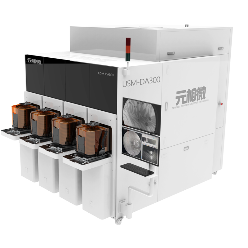
DI-USM (High Throughput Electron Beam Wafer Inspection Equipment)
The application of surface quantum microscopy technology for large field of view, high-throughput, and high-resolution imaging of silicon wafer surfaces, and the detection of surface electrical and physical defects through image big data processing and AI algorithms, is a key equipment for improving yield in chip manufacturing processes.
- Ultra high throughput
- high resolution
- Tomographic detection
- Element discrimination
- Band analysis
- Growth dynamics (ALD/CVD/MBE)
- K-space distinguish
- High temperature in-situ