Application Scenarios
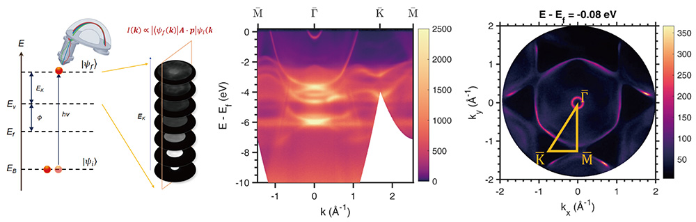
With momentum space imaging technique, USM-SPE is able to image the whole upper hemispherical photoemission horizon of a sample. The acquired data is momentum image I(k, k) with different electron kinetic energies, which are stacked to from a 3D dataset I(E, k, k). The result can be obtained by slicing out at any direction . In addition, USM-SPE can select a small area in the sample space for μ-ARPES analysis for high-quality data.
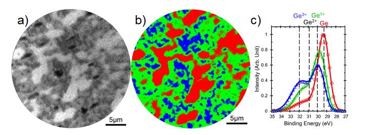
USM-SPE is a powerful tool for aging and corrosion analysis. USM-SPE can analyse the spatial distribution of elements and chemical states at high resolution (≤ 50 nm). The oxidation process of Ge(110) surface can be visualized by chemical distribution map (left) and the corresponding spectrum (right).
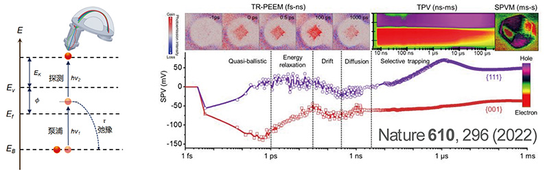
Combined with pump-probe technique, USM-SPE enables the observation of ultrafast charge transfer and relaxation process on femtosecond to nanosecond time scales. This detailed processes provides unprecedented insights into the diagnosis of charge separation in photocatalysis and is essential for the design of efficient photocatalysts.
In-situ chemical vapor deposition (CVD) offers significant advantages in material growth and characterization, especially in two-dimensional materials and applications in electronics, energy, and nanotechnology. USM-E in-situ characterization technology provides a powerful tool for real-time monitoring and analysis of materials. This technology enables real-time observation of material growth and structural changes during deposition, providing instant feedback to optimize deposition parameters and improve thin film quality.
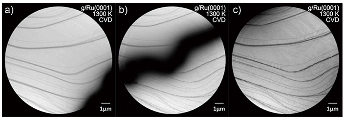
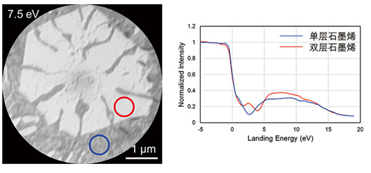
In the field of nanomaterials and 2D materials research, accurate calibration of atomic-scale thin film layers is a key technological bottleneck to achieve performance tuning. USM-E is able to resolve the thickness and number of layers of thin films through its unique surface-sensitive electron interferometry technology. USM-E can accurately determine the monolayer closure of epitaxial growth and capture defect-induced local layer variations during film deposition (e.g., CVD, MBE) or etching processes. USM-E provides a standardized platform for calibrating the number of layers of ultrathin films with sub-Angstrom-level vertical resolution and nanometre-level lateral resolution for research and development, laboratory exploration to industrial production, integration.