Product Center
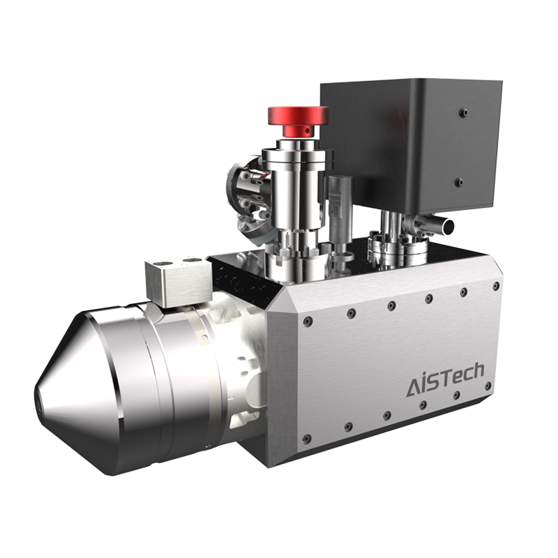
Microbeam EUV, X-ray light source
Microbeam EUV and X-ray light sources have been developed for advanced semiconductor process inspection. Stabilized micro-spots are produced by precise bombardment of high-purity targets with electron beam, generating high-resolution images for more intuitive results. This product is mainly used for thin film inspection or 3D packaging inspection.
Specifications
| Specifications | |
|---|---|
| Electronic acceleration voltage |
15 kV~20kV (EUV) 40 kV~60kV (X-ray) |
| Target material | Silicon(EUV);Tungsten(X-ray) |
| Spot size | ≥200 nm |