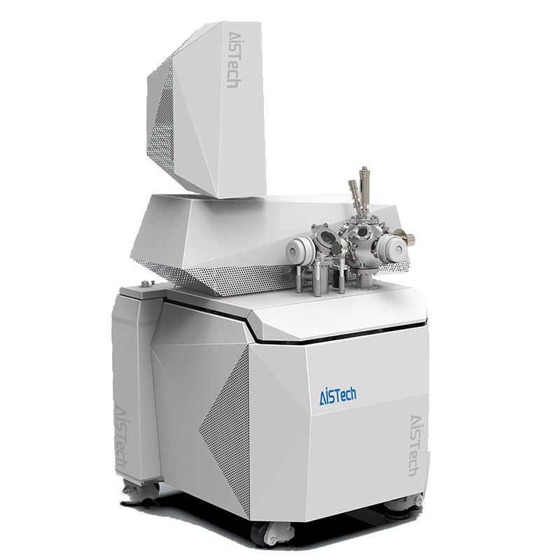
USM-E Electron Microscope
is a multifunctional, high-performance surface analyser that can be used for in-situ observation of kinetic processes on the surface of solid material samples such as surface growth, phase transitions, diffusion, doping. The product can in turn be used in holographic surface analysis systems to achieve sub-monolayer sensitivity measurements. It has a wide range of applications in the fields of ultra-thin film growth, two-dimensional materials, metals, semiconductors, magnetic materials, and nanomaterials.
Specifications
|
Specifications
|
|
Cathode
|
Schottky hot field emitter/spin-polarized emitter
|
|
Resolution
|
≤ 5 nm
|
|
Field of view
|
1 μm – 160 μm
|
|
Sample temperature
|
10 K – 2000 K
|
|
Degree of vacuum
|
Spin polarized cathode:≤1x10-11mbar
Main Chamber:≤ 1×10⁻¹⁰ mbar
|
Imaging mode and mechanism
|
Imaging mode
|
|
(SP)LEEM
|
|
(SP)LEED, μ(SP)LEED
|
|
MEM
|
|
ps-(SP)LEEM/(SP)LEED
|
|
Imaging mechanism
|
|
Bright field, dark field
|
|
Magnetism
|
|
Quantum phase
|
|
Reflectance
|